Laboratory of Physics of Nanostructures
Laboratory of Physics of Nanostructures specializes in its research and teaching in materials science and the physics of low-dimensional structures and their applications. In addition, the laboratory has very good engineering and technological competence.
Main directions of research
- Nanotribology (or nanoparticle interactions)
- Material technology (we study thermoplastics and wood - for example plywood)
- Surface treatment (coating of wood and metal with various functional films)
Cooperation
Laboratory of Physics of Nanostructures has different partners both inside and outside of the institute: Laboratory of Laser Spectroscopy, Laboratory of X-Ray Spectroscopy, Institute of Chemistry, Institute of Technology, TalTech. Entrepreneurial co-operation is also actively pursued (e.g. Andrese Klaasi AS, Otepää Kymmene OÜ, KuMa Wood OÜ, Nordfix OÜ).
|
Rünno Lõhmus
|
|
|
Kristjan Saal
|
|
|
Sergei Vlassov
|
|
|
Sven Oras
|
|
|
Madis Lobjakas
|
PRG1198 "Development of laser-based pen-type probe-MS system for the analysis of cultural heritage objects (1.01.2021−31.12.2025)", Signe Vahur, University of Tartu, Faculty of Science and Technology, Institute of Chemistry.
PLTFYARENG53 "Development of antimicrobial surface coatings tested in real-life conditions into pilot production phase (18.02.2021−31.12.2021)", Vambola Kisand, University of Tartu, Faculty of Science and Technology, Institute of Physics.
LLTFY21434 (2014-2020.4.02.21-0348) "Reusable monopolymeric plastic packages (1.07.2021−27.12.2023)", Sven Lange, University of Tartu, Faculty of Science and Technology, Institute of Physics.
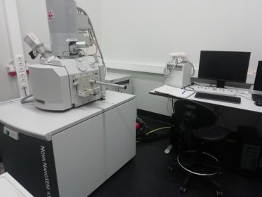
Scanning electron microscope Nova NanoSEM 450 (FEI)
- Resolution 1.4 nm.
- Can be used to measure in low-vacuum regime and visualize non-conducting samples (glasses, ceramics, wood).
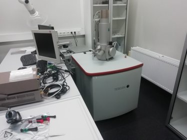
Scanning electron microscope Vega II SBU (Tescan)
- Useful for quick visualization of samples; ideal for fast characterization of the surface features of samples (cracks, surface roughness); does not have high resolution.
- Easy to use, good for learning the basics of electron microscopy.
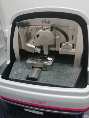
Atomic Force Microscope Dimension Edge (Veeco)
- This device allows high resolution with conducting and non-conducting samples.
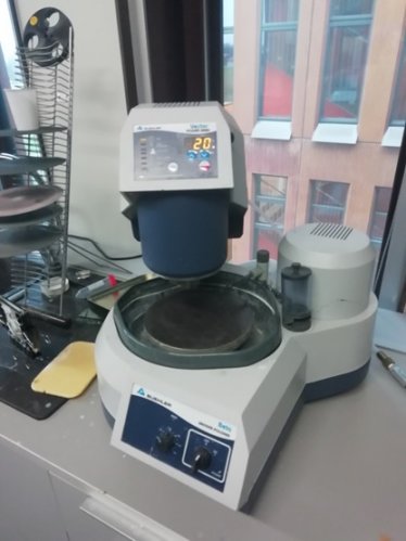
Buehler Beta Grinder Polisher
- Can be used for polishing of the samples to desired surface roughness.
- Useful for preparation of samples for microscopy when it is necessary to examine the interior of a delicate test object (biological tissue, fragile minerals) The test object is immersed in a two-component polymer (epoxy) and after the hardening of polymer, sanded to the desired surface roughness. The obtained cross-section allows to visualize the inside of the test object (optical, atomic force, electron microscopy).